- 您现在的位置:买卖IC网 > Sheet目录344 > MSL2100BR (Atmel)IC LED DRIVER 8 STRING
��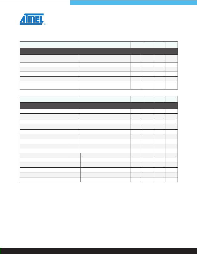 �
�
�PARAMETER�
�CONDITIONS� AND� NOTES�
�MIN�
�TYP�
�MAX�
�UNIT�
�AC� ELECTRICAL� CHARACTERISTICS�
�OSC� initial� accuracy�
�PHI� frequency�
�GSC� frequency�
�PWM� frequency�
�PWM� duty� cycle�
�f� OSC�
�f� PHI�
�f� GSC�
�f� PWM�
�OSCCTRL� =� 0x04� (f� OSC� =20MHz);�
�T� A� =25°C�
�(Note� 7)�
�(Note� 7)�
�PWMDIRECT� =� PWMEN� =� 1�
�PWMDIRECT� =� PWMEN� =� 1�
�18�
�40�
�20�
�0�
�20�
�22�
�10,000�
�5�
�50,000�
�100�
�MHz�
�Hz�
�MHz�
�Hz�
�%�
�PHI� DLL� lock� cycles�
�4�
�PHI�
�Cycles�
�PARAMETER�
�CONDITIONS� AND� NOTES�
�MIN�
�TYP�
�MAX�
�UNIT�
�I2C� SWITCHING� CHARACTERISTICS�
�SCL� clock� frequency�
�1/t� SCL�
�Bus� timeout� disabled� (Note� 1)�
�0�
�1,000�
�kHz�
�Bus� timeout� period�
�t� TIMEOUT�
�OSCCTRL� =� 0x04� (f� OSC� =20MHz);� T� A� =25°C�
�27�
�30�
�33�
�ms�
�STOP to START condition bus free time�
�Repeated� START� condition� hold� time�
�Repeated START condition set-up time�
�STOP� condition� set-up� time�
�SDA� data� hold� time�
�t� BUF�
�t� HD:STA�
�t� SU:STA�
�t� SU:STOP�
�t� HD:DAT�
�0.5�
�0.26�
�0.26�
�0.26�
�15�
�μs�
�μs�
�μs�
�μs�
�ns�
�SDA� data� valid� acknowledge� time�
�SDA� data� valid� time�
�SDA� data� set-up� time�
�SCL� clock� low� period�
�SCL� clock� high� period�
�SDA,� SCL� fall� time�
�SDA,� SCL� rise� time�
�SDA,� SCL� input� suppression� filter� period�
�t� VD:ACK�
�t� VD:DAT�
�t� SU:DAT�
�t� LOW�
�t� HIGH�
�t� F�
�t� R�
�t� SP�
�(Note� 2)�
�(Note� 3)�
�(Note� 4,� Note� 5)�
�(Note� 6)�
�0.05�
�0.05�
�100�
�0.5�
�0.26�
�50�
�0.55�
�0.55�
�120�
�120�
�μs�
�μs�
�ns�
�μs�
�μs�
�ns�
�ns�
�ns�
�10�
�Note1.�
�Note2.�
�Note3.�
�Note4.�
�Note5.�
�Note6.�
�Note7.�
�Note8.�
�Note9.�
�Minimum� SCL� clock� frequency� is� limited� by� the� bus� timeout� feature,� which� resets� the� serial� bus� interface� if� either� SDA� or� SCL� is� held� low� for�
�t� TIMEOUT� .� Disable� bus� timeout� feature� for� DC� operation�
�t� VD:ACK� =� SCL� low� to� SDA� (out)� low� acknowledge� time�
�t� VD:DAT� =� minimum� SDA� output� data-valid� time� following� SCL� low� transition�
�A� master� device� must� internally� provide� an� SDA� hold� time� of� at� least� 300ns� to� ensure� an� SCL� low� state�
�The� maximum� SDA� and� SCL� rise� times� are� 300ns.� The� maximum� SDA� fall� time� is� 250ns.� This� allows� series� protection� resistors� to� be�
�connected� between� SDA� and� SCL� inputs� and� the� SDA/SCL� bus� lines� without� exceeding� the� maximum� allowable� rise� time�
�The� MSL2100� includes� input� filters� on� SDA,� SCL,� AD0,� and� AD1� inputs� that� suppress� noise� less� than� 50ns�
�Parameter� is� guaranteed� by� design,� and� is� not� production� tested�
�Subject� to� thermal� dissipation� characteristics� of� the� device�
�When� mounted� according� to� JEDEC� JEP149� and� JESD51-12� for� a� one-layer� PCB,� θ� JA� =� 22°C/W� and� θ� JC� =� 1.3°C/W�
�Atmel� LED� Driver-MSL2100�
�发布紧急采购,3分钟左右您将得到回复。
相关PDF资料
MSL2160DQ
IC LED DRIVER 16 STRING
MSL2162DQ
IC LED DRIVER 16 STRING
MSL3082CS
IC LED DRIVER 8 STRING
MSL3085BT
IC LED DRIVER 8 STRING
MSL3162BT
IC LED DRIVER 16 STRING
MSL3164BT
IC LED DRIVER 16 STRING
MSL3167GU
IC LED DRIVER 16 STRING
MT-6 PLUS
SURGE SUPPR TCHMSTR 6OUT 10'CORD
相关代理商/技术参数
MSL2100BR-R
功能描述:LED照明驱动器 8 Str Hi Pwr, White or RGB LED Drivers
RoHS:否 制造商:STMicroelectronics 输入电压:11.5 V to 23 V 工作频率: 最大电源电流:1.7 mA 输出电流: 最大工作温度: 安装风格:SMD/SMT 封装 / 箱体:SO-16N
MSL2160
制造商:未知厂家 制造商全称:未知厂家 功能描述:16-string, White and RGB LED Drivers with Adaptive Configuration,EEPROM, and SPI/I2C/SMBus Serial Interface
MSL2160DQ
功能描述:LED照明驱动器 16-StringRGBLED Dvrs AdapPwrContr E2Prom
RoHS:否 制造商:STMicroelectronics 输入电压:11.5 V to 23 V 工作频率: 最大电源电流:1.7 mA 输出电流: 最大工作温度: 安装风格:SMD/SMT 封装 / 箱体:SO-16N
MSL2160DQ-R
功能描述:LED照明驱动器 16String White & RGB LED Drivers with A
RoHS:否 制造商:STMicroelectronics 输入电压:11.5 V to 23 V 工作频率: 最大电源电流:1.7 mA 输出电流: 最大工作温度: 安装风格:SMD/SMT 封装 / 箱体:SO-16N
MSL2161
制造商:ATMEL 制造商全称:ATMEL Corporation 功能描述:16-string, White and RGB LED Drivers with Adaptive Configuration, EEPROM, and SPI/I2C/SMBus Serial Interface
MSL2161DQ
功能描述:LED照明驱动器 16String White & RGB LED Drivers with A RoHS:否 制造商:STMicroelectronics 输入电压:11.5 V to 23 V 工作频率: 最大电源电流:1.7 mA 输出电流: 最大工作温度: 安装风格:SMD/SMT 封装 / 箱体:SO-16N
MSL2161DQ-R
功能描述:LED照明驱动器 16String White & RGB LED Drivers with A RoHS:否 制造商:STMicroelectronics 输入电压:11.5 V to 23 V 工作频率: 最大电源电流:1.7 mA 输出电流: 最大工作温度: 安装风格:SMD/SMT 封装 / 箱体:SO-16N
MSL2162DQ
功能描述:LED照明驱动器 16-String RGBWhite LED Dvrs AdapCon E2P RoHS:否 制造商:STMicroelectronics 输入电压:11.5 V to 23 V 工作频率: 最大电源电流:1.7 mA 输出电流: 最大工作温度: 安装风格:SMD/SMT 封装 / 箱体:SO-16N